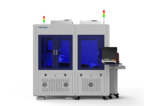
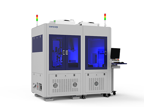
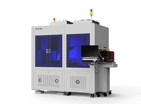
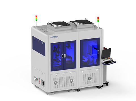
Product Description
Cencorp 1200AW is used for surface macro defect inspection of wafer and substrate/post die bonding during the semi-conductor assembly and test stage. It supports automatic loading and unloading of 8-inch/12-inch wafer and substrate/post die bonding device, and is manually compatible with surface macro defect inspection of 12-inch wafer after dicing and single chip.
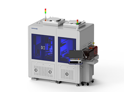
Advantages
Take into account the defect inspection of various process nodes in the chip assembly and test stage, including wafer incoming inspection before dicing, wafer inspection after dicing, substrate inspection, post die bonding device, and single chip inspecti