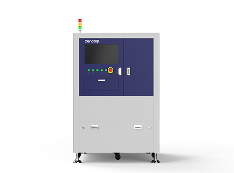
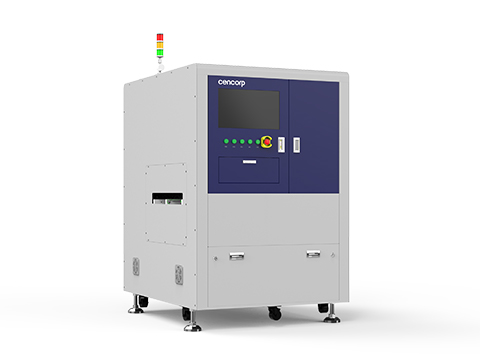
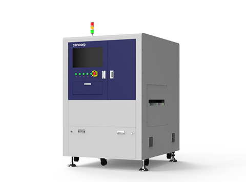
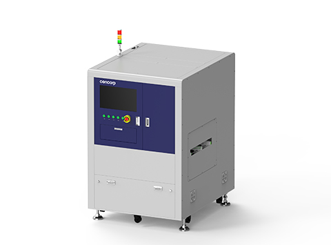
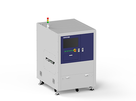
Product Description
The wafer surface film thickness measurement equipment (Film1000) is a high-precision, non-contact system designed for accurate measurement of thin films on semiconductor wafers (e.g., silicon and compound semiconductors). Utilizing optical interference and spectral analysis technologies, combined with a high-resolution imaging system and intelligent algorithms, the device enables nanoscale thickness measurements of metal layers, oxides, nitrides, photoresist, and more.
Advantages
High-Precision Measurement: Sub-nanometer resolution meets advanced process control requirements.
Multi-Layer Detection: Simultaneously measures stacked films of different materials.
Non-Contact Inspection: Prevents sample damage, suitable for precision w